Tutorial
Using Microvolt
To use Microvolt you should include sc_ui.h file to your code
#include "sc_ui.h"
Microvolt should be initialized with command line arguments
int main(int argc, char **arv){
 scInit(argc,argv);
 ...              // your code
 return 0;
}
Function scInit has 3rd optional argument where you can specify directory for output files. This arguments is empty string by default (this means that all files are recorded to directory with your executable file).
Geometry objects
We are using ivutils library to construct geometry objects. Please read description here.
Media
Medium is constructed by structure scMediumFactory which is declared in sc_mediumfactory.h. To specify medium you need to assign following variables of scMediumFactory:
- eps – dielectric permittivity
- Eg, chi – bandgap and electron affinity, eV
- dop - doping concentration (positive for n-doping, negative for p-doping), cm-3
- T – temperature, K
- mu[2] – electron and hole mobilities, cm2V-1s-1
- m[2] - effective electron (hole) mass relative to electron mass in vacuum
- N[2] effective density of states in conduction (valence) band, cm-3
- rcm - object of structure scRecomb which stores parameters for different types of recombination
Parameters m and N are related to each other. If you specify N, then m will be expressed via N. If you specify m only (N is zero), then N will be expressed via m.
Structure scRecomb stores following parameters:
Radiative recombination:
- B – capture probability, cm3s-1
Auger recombination:
- C[2] - capture probability, cm6s-1
Shockley-Reed-Hall recombination with single trap layer (we didn’t implement multiple trap layers, however, this can be done easily):
- trap - difference between tap layer and intrinsic Fermi level, eV
- tau[2] – lifetime of the minority electrons (holes) in the p(n)-region, s
In sc_mediumfactory.h we declare functions that construct objects scMediumFactory for some semiconductors (Si, a-Si, GaAs, Ge, CdTe, CdS). The only argument of these functions is binary flag that specify which types of recombination should be turned on / off. Default value of this argument is zero. For example
scMediumFactory med = getscSi();
corresponds to silicon with zero parameters for all types of recombination.
scMediumFactory med = getscSi(recombRad| recombAuger | recombSRH);
corresponds to silicon with predefined parameters for all types of recombination. B and C values are taken from literature, whereas SRH recombination is assumed to be produced by single-trap level at the intrinsic Fermi level with life time for electrons and holes equal to 10-7s.
Numerical experiment
Generally, in order to perform numerical experiment, you need to specify: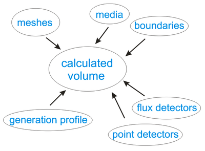
- Calculated volume and mesh resolution. Multiple meshes with different resolution can be used.
- Material properties and geometry of the structure.
- Boundary conditions (contacts and insulator interfaces).
- Carriers’ generation profile (if you simulate solar cells). Generation profile can be obtained using Beer's law or taken from independent electromagnetic modeling.
- Set of points ("detectors") where calculated variables (electrostatic potential, electrons and holes concentration and current, etc.) are recorded to output text files.
- Imaginary surfaces to measure current flux.
During simulation, you find equilibrium solution for zero applied voltage, then increase voltage gradually in steps of dV, and find solution for each voltage value. Detectors produce output text files with calculated variables. You can also calculate current flux through chosen surfaces that can be used to plot IV-curve.
Below we illustrate this on the example of 1D diode.
1D diode (solar cell)
Here we show how to simulate one-dimensional silicon diode.
Length of diode is 1 micron.
valtype length=1; // diode length, micron
Calculated volume is box with opposite corner coordinates (0,0,0) and (0,0,d).
We consider 1D problem, and specify nonzero size only for z dimension.
The main class for numerical experiment is uiExperiment declared in sc_ui.h. Let’s make object of this class and specify calculated box.
uiExperiment task(Vector_3(0,0,0),Vector_3(0,0,length));
Now we should call functions of this object to specify geometry and perform a simulation.
In Microvolt length unit is 1 micron by default. However, it can be changed by function SetLengthUnit with new length unit in microns as a parameter.
We will use mesh step 0.001 microns
valtype dr=0.001;
task.SetResolution(dr);
Medium regions
We simulate silicon diode with doping concentration 1018 cm-3. We consider only SRH recombination from a single-trap level at intrinsic Fermi level and choose the lifetime of the minority electrons in the p-region equal to the lifetime of minority holes in the n-region \(\tau_{n} = \tau_{p}\).
We will specify these lifetimes indirectly via minority electrons diffusion length \(L_n=\sqrt{\tau_n D_n}\). It is easier to operate with diffusion length rather than with lifetime and other recombination parameters, since diffusion length gives the idea of the recombination length scale compare to device size.
Including Auger and radiative recombination results primarily in a change the diffusion length Ln. Rather than adding these other recombination channels into the microscopic expression for recombination, for simplicity we subsume these processes into the overall diffusion length Ln.
scMediumFactory left_med=getscSi(), right_med=getscSi(); left and right media
L_n=1; // diffusion length, microns
left_med.L[0]=right_med.L[0]=L_n;
left_med.dop=1e18, right_med.dop=-1e18; // left and right doping concentrations, cm-3

valtype left_length=.01; // pn-junction position, microns
task.AddMediumRegion(left_med,GetHalfSpace(-n,left_length*n));
task.AddMediumRegion(right_med,GetHalfSpace(n,left_length*n));
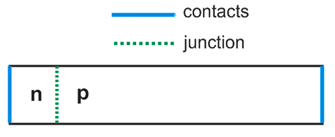
First argument of AddMediumRegion is scMediumFactory, second argument is doping (positive value corresponds to n-doping; negative value corresponds to p-doping), third argument is region where medium is placed. Space at the left from pn-interface is occupied by n-doped silicon, and at the right – by p-doped silicon.
Contacts
We use Ohmic contacts with surface recombination 105 cm/s.
valtype sr=1e5; // surface recombination, cm/s. VEC_INFTY indicates infinite surface recombination
valtype wf=VEC_IFNTY; // contact workfunction for Schottky contact, eV. VEC_INFTY indicates Ohmic contact
task.AddContact(GetHalfSpace(-n,VEC_ZERO*n),sr,sr,wf);
task.AddVoltageContact(GetHalfSpace(n,(length-VEC_ZERO)*n),sr,sr,wf);
First argument of the function corresponds to region where contact is placed. With given choice of regions, first and last nodes of 1D mesh belong to left and right contacts (VEC_ZERO is very small positive constant). In general, all mesh boundary nodes should be covered by contact, insulator interface or some other mesh.
Second (third) argument is surface recombination values for electrons (holes), cm/s. If it is equal to VEC_INFTY, than surface recombination is infinite that correspond to equilibrium concentration of carriers at the contact. Fourth argument is workfunction for Schottky contact, eV. In order to model Ohmic contact we specify VEC_INFTY value for workfunction.
Using ‘Voltage’ in name of the second function means that we are planning to apply voltage to the second contact (we will discuss this later).
Detectors
Our next step is to specify points where calculated variables (electrostatic potential, electrons and holes concentration, current, etc.) will be recorded to output text files. We call them detectors.
task.AddDetector("d",0,sz,iVector_3(1,1,length/dr+1));
First parameter of AddDetector is detectors name (“d” in our case) which will be used for output text filed. Next three parameters specify 3D grid where detectors are placed, namely, two opposite corners of the grid and number of grid steps along three directions.
We will also calculate current flux through planar section of the diode.
AddFluxPlane("j",2,length);
This planar section is normal to z direction and crosses z-axis at coordinate length.
Calculation
To start a simulation we should call:
task.Calculate();
Now code is ready, you can compile and run it. During execution program reports the calculation status. If something is wrong, then you will get corresponding message and function Calculate will return -1.
Calculation consists in looking for solution of Poisson equation ("p") and continuity equations for electrons and holes ("eh") by Newthon-Rhapson iterations which minimize residue values for these equations. While solving each equation(s), program displays three numbers which are residue values for Poisson equation, for continuity equation for electrons and for continuity equation for holes. You can also see old and new residues for equation which is currently solving:
‘equation_type_(e_or_eh) residue_p residue_e residue_h old_residue -> new_residue’.
If Newthon-Rhapson method get stuck and residue does not change, than you will see sign '<->'. Two signs ‘<->’ ahead for Poisson and continuity equations mean that residue minimum is achieved. If this residue is small enough then you get the solution. Otherwise, you arrived to a local (not global) residue minimum, and you need to change the method of solution or use better mesh. We will discuss these options later.
Number of iterations is limited by some maximal value. By default this is 50, but it could be changed manually. Calculation will be stopped after number of iterations will reach this value even if residue minimum is still not achieved.
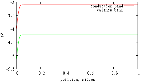
In output file ‘d.d’ you can find values of calculated variables at detectors:
- electrostatic potential (psi), eV
- quasi Fermi level for electrons (fermin), eV
- quasi Fermi level for holes (fermip), eV
- conduction band (cond), eV
- valence band (val), eV
- electrons concentration (n), cm-3
- holes concentration (p), cm-3
- doping concentration (dop), cm-3
- recombination rate ( R ), s-1cm-3
- generation rate (G), s-1cm-3
- electrons current density (Jn), A/cm2
- holes current density (Jp), A/cm2
You can plot data from this file using popular gnuplot program.
For example, to plot conduction and valence bands you should open gnupolt, move to directory with ‘d.d’ file using cd command (specify directory name in quotes) and type
gnuplot> set xlabel 'position, micron'
gnuplot> set ylabel 'eV'
gnuplot> p 'd.d' u 1:5 w l t 'conduction band', 'd.d' u 1:6 w l t 'valence band'
File 'j.d' shows how current flux through chosen planar surface depends on applied voltage. Since we performed simulation only for zero voltage, this file has only one value there which is zero.
We can simulate nonzero voltages:
task.Calculate(.02,.2);
In this example we simulate all voltages from 0 to .2 with step .02.
Calculated IV-dependence in file 'j.d' can be plotted in gnuplot:
gnuplot> set xlabel 'voltage, V'
gnuplot> set ylabel 'current, A/cm2'
gnuplot> p 'j.d' w l
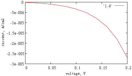
We will also find bunch of files 'dxxx.d' with calculated variables for each voltage xxx.
Carriers' generation
Carrier’ generation is produced by absorbed photons with energy higher than semiconductor bandgap. Generation leads to appearance of photocurrent in solar cells.
In Microvolt generation is constructed by class scGeneration or any of its inheritors (scGenerationTable, scLambert, scLambertSpectrum, etc.) which correspond to different ways to specify generation. To use some particular generation you need to call function AddGeneration.
In general, photons absorption and generation should be calculated by independent electromagnetic simulation. This generation can be substituted to Microvolt using class scGenerationTable which will be described later when we will consider 3D geometries.
In our simple 1D case we can calculate generation using Lambert-Beer law for absorption in homogeneous media and assuming no reflection from front (perfect antireflective coating) and back sides of the cell:
\(R(z) = I \alpha e^{-\alpha z}\),
where I is incident photon flux, \(\alpha\) is the absorption coefficient.
For example, incident light of intensity 1020s-1m-2 enters the cell at the left side. The absorption coefficient is 1m-1. In this case we can use class scLambert:
Vector_3 n(0,0,1);
scGeneration *gen = new scLambert(Plane_3(n,0), 1e20, 1);
task.AddGeneration(gen);
First parameter of scLambert constructor is plane where light enters the cell, second is light intensity and third is absorption coefficient \(\alpha\).
Absorption coefficient can be expressed through imaginary part of refractive index \(\alpha = 4\pi k/\lambda\).
We keep files with optical data for different semiconductors in the directory ‘spectra’ (“si.nk”, “cds.nk”, “cdte.nk”, etc.). Data in these files is presented in tabular format wavelength – n (real part of refractive index) – k (imaginary part of refractive index). Absorption coefficient can be calculated using tabular data in some *.nk file.This is example for 500nm monochromatic light of intensity 103Wm-2 which propagates in silicon diode:
const char *spectra_dir = “”;
scGeneration *gen =  scLambert(Plane_3(n,0),1e3,500,spectra_dir,"si.nk");
task.AddGeneration(gen);
Fourth parameter of used scLambert constructor is path to directory ‘spectra’ (you need to choose path accordingly to location of this directory on your machine).
If incident light covers some spectral range and \(\alpha\) depends on a wavelength, than generation rate can be calculated as:
\(G(z) = \int_{\lambda_{\rm min}}^{\lambda_{\rm min}} \frac{\lambda}{hc} I(\lambda) \alpha e^{-\alpha z} d\lambda\),
where \(I(\lambda)\) is incident spectral density, W/m2/nm.
To specify this type generation, you can use class scLambertSpectrum:
valtype wv1 = 350; // shortest wavelength that enters the cell
valtype wv2 = 1240.8/left_med.Eg; // wavelengths that corresponds to silicon bandgap
scGeneration *gen =  scLambertSpectrum(Plane_3(n,0),spectra_dir,"am1.5.in","si.nk",left_med.Eg);
task.AddGeneration(gen);
In this example incident light spectrum is taken from “am1.5.in” file in a wavelength range (wv1, wv2). File "am1.5.in" contains data for solar Air Mass 1.5 Global Spectrum in tabular format wavelength – intensity, W/m2/nm.
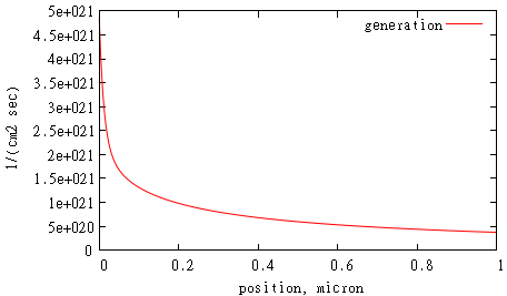
Let’s perform a simulation using this last choice of carrier’s generation.
This is the shape of generation profile inside the cell:
gnuplot> set xlabel 'position, micron'
gnuplot> set ylabel '1/(cm2 sec)'
gnuplot> p 'd.d' u 1:11 w l t 'generation'
It makes sense to run a calculation until voltage exceeds open circuit voltage value. This moment can be detected when current flux through some surface changes sign while we increase voltage by dV. We can choose surface “j” for this purpose:
task.SetFluxIV("j");
If we call Calculate with first argument only
task.Calculate(0.02);
then calculation will stop when current flux through this surface changes the sign. It can be shown from obtained IV-curve (we don’t connect calculated values by lines in order to make it clear)
gnuplot> set xlabel 'voltage, V'
gnuplot> set ylabel 'current, A/cm2'
gnuplot> p 'j.d', 0
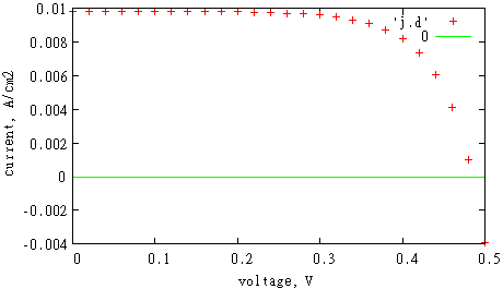
Open circuit voltage is obtained by linear interpolation between two voltages V and V+dV with opposite current values. In order to improve accuracy of calculated open circuit voltage, one can use smaller dV.
As a result of simulation, we will get file 'sc.dat' with following data: surface area s, short circuit current J, short circuit current density Jsc =J/s, open circuit voltage Voc, filling factor, maximal power, efficiency which is calculated as maximal power divided by AM1.5 solar spectrum intensity and surface area. In our case we got Jsc = 0.01 A/cm2, V = 0.48 V. This is in a good agreement with results obtained for the same geometry in paper by B. M. Kayes, H. A. Atwater, and N. S. Lewis, "Comparison of the device physics principles of planar and radial p-n junction nanorod solar cells," J. Appl. Phys., 97, 114302 (2005).
Nonuniform mesh step
Carriers’ concentration changes more rapidly near junction area (and sometimes near contacts). Resolution there should be sufficiently high to resolve these changes. Far from junction area carriers’ concentration doesn’t change significantly and resolution can be smaller. Here we show how to vary resolution in our example with 1d diode. We will use mesh step 0.001 micron only around junction, and use smaller mesh step 0.01 micron elsewhere. To generate such nonuniform mesh we use function generate_1d_mesh.
vector<Vector_3> inc;
inc.push_back(Vector_3(0,2*left_length,dr/10));
vector<valtype> mesh;
if(generate_1d_mesh(Vector_3(0,length,dr),inc,mesh)<0)
return -1;
task.SetMeshSteps(2,mesh);
The idea of our nonuniform mesh generator is to take some initial global mesh with small resolution, insert some local meshes with high resolution, and make continuous transition of the mesh step between these meshes. First parameter of generate_1d_mesh describes small resolution mesh: left node is 0, right node is d, and mesh step is dr. Second parameter is vector where you put descriptions of high resolution meshes that will be inserted within rough mesh. We have only one high resolution mesh, its left node is 0, right node is 2*left_length, and mesh step is dr/10. Function generate_1d_mesh stores generated nonuniform mesh nodes in third parameter which is vector. If something is wrong with first two parameters, it returns -1. We call SetMeshSteps to apply generated nonuniform mesh nodes at z-direction (which is fist argument of this function). Note that in 2d and 3d cases you can call SetMeshSteps for each direction separately.
To see mesh nodes position and values of calculated variables there you can call.
task.DumpMeshes();
After calculation you will get files ‘m.d’ similar to detectors files.
gnuplot> p [:.2] 'm.d' u 1:5, ‘m.d’ u 1:6
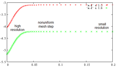
One can see that bands level changes mostly around junction area, where we use high resolution mesh.
We calculated IV-curve for different resolution setups: (1) uniform mesh with dr=0.001 (as we used before), (2) uniform mesh with dr=0.01, and (3) generated nonuniform mesh with 0.001 step around junction and 0.01 elsewhere.
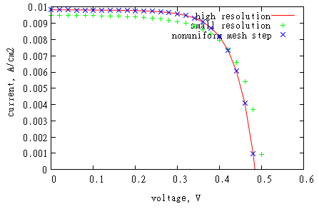
One can see that using high resolution around junction area only gives same results as using high resolution everywhere. Using nonuniform mesh can save memory and time
resources. Usually open-circuit voltage value is more sensitive to using high resolution around junction that short circuit current.
Heterojunctions, alloys
This section is under development.
I am planning to finish it at the end of November.
Multi-dimensional devices
2D multilayer cell
To absorb all the incident light, thickness of the planar silicon solar cell should be of hundreds of microns. It leads to cost issues caused by need of silicon of high quality to extend diffusion length and collect generated carriers before they can recombine. To avoid the problem associated with need of high quality silicon, multilayer solar cells could be used. Multilayer cell consists in a number of parallel n and p layers with a thickness of the order of silicon diffusion length. In this cell generated carriers remain close to pn-junction and get collected before they can recombine.
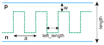
Here we show how to simulate 2D multilayer using Microvolt. All used dimensions are showed at the image below. Case w=length/2 corresponds to the planar diode.
int main(int argc,char **argv){

  string dir; // output directory
  if(scInit(argc,argv,dir)<0)
    return -1;

  valtype length=2; // diode vertical length
  valtype w=.2; // pn-junction position along diode length
  valtype a=1; // period
  valtype left_length=.4; // width if the layer

  int hp=2; // number of half-periods in calculated box

  valtype ndop=1e18; // n doping concentration, cm-3
  valtype pdop=-1e18; // p doping concentration
  valtype L=1; // diffusion length, mkm
  valtype sr=1e5; // surface recombination, cm/sec

  valtype dy=.02;
  valtype dz=.02;

  scMediumFactory left=getscSi(); // silicon
  scMediumFactory right=left;
  left.L[0]=right.L[0]=L;
  left.dop=ndop;
  right.dop=pdop;

  Vector_3 sz(0,hp*a/2,length);
  scExperiment task(0,sz);
  task.SetResolution(Vector_3(0,dy,dz));

  task.AddMediumRegion(right,new Region_3(),-1); // default medium
  if(accomp(w,length-w)) // planar diode case
    task.AddMediumRegion(left,GetHalfSpace(Vector_3(0,0,-1),w));
  else{
    for(int i=0;i<=hp;i+=2)
      task.AddMediumRegion(left,GetPlate(Vector_3(0,1,0),-.5*left_length+i*a/2,left_length));
    task.AddMediumRegion(left,GetHalfSpace(Vector_3(0,0,-1),w),1);
    task.AddMediumRegion(right,GetHalfSpace(Vector_3(0,0,1),length-w),1);
  }

  task.SetPeriodicBoundaries(0x2); // set periodicity for y-dimension

  Region_3 *BR = GetHalfSpace(Vector_3(0,0,-1),VEC_ZERO);
  Region_3 *UR = GetHalfSpace(Vector_3(0,0,1),length-VEC_ZERO);

  task.AddContact(BR,sr,sr,VEC_INFTY);
  task.AddVoltageContact(UR,sr,sr,VEC_INFTY);

  task.AddDetector("d",0,sz,iVector_3(1, hp*10, 20));

  task.AddFluxPlane("j",2,sz[2]/2);

  task.AddGeneration(new scLambertSpectrum(Plane_3(Vector_3(0,0,1),0),spectra_dir.c_str(),
    "am1.5.in","si.nk",350,1240.8/left.Eg));

  task.SetFluxIV("j");
  task.Calculate(.02);

  return 1;
}
Note that you can specify arbitrary number of half-periods (hp) inside the calculated box. We use hp=2 to simulate one period.
While specifying pn-junction geometry we use last parameter of AddMediumRegion which corresponds to the region priority: if two medium regions intersect, medium with higher priority is simulated.
We use periodic boundary conditions for y-direction, and confine cell by contacts in z-direction. X-direction is not working.
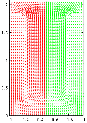
This is resulted photocurrent distribution (zero voltage), see left figure. Note that we multiply value of the current density on 3 (mult=3) for better visualisation
gnuplot> mult=3
gnuplot> p [0:1][0:2.5] 'd.d' u 1:2:(mult*($13+$15)):(mult*($14+$16)) w vec
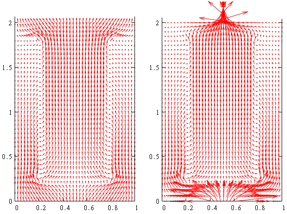
One can see that current flows from bottom contact to top contact through pn-interface.
In files ‘j.d’ and ‘sc.dat’ you can find IV-characteristic and other parameters of simulated solar cell (see detailed description in 1D diode example).
Efficiency of solar cell can be improved by reducing the influence of surface recombination at the contacts.
It can be done by using highly doped region near contacts (surface field).
The interface between the higher and lower doped regions behaves like a p-n junction where the resulting electric field makes a potential barrier to minority carrier flow to the surface.
Another way to eliminate recombination at the contacts is to reduce directly contacts area and passivate the rest surface with silica. Below we demonstrate second approach, modifying contacts position:
// Region_3 *BR = GetHalfSpace(Vector_3(0,0,-1),VEC_ZERO);
// Region_3 *UR = GetHalfSpace(Vector_3(0,0,1),length-VEC_ZERO);

// task.AddContact(BR,sr,sr,VEC_INFTY);
// task.AddVoltageContact(UR,sr,sr,VEC_INFTY);

 valtype sri=1e2; // insulator surface recombination, cm/sec
 valtype cwidth = .2; // dot contact width
 Polyhedron_3 *conf = GetPlate(Vector_3(0,1,0),(sz[1]-cwidth)/2,cwidth);
 task.AddVoltageContact(new ConfinedRegion<Region_3>(BR,conf),sr,sr,VEC_INFTY,1);
 task.AddReflectiveBoundary(BR,sri,sri);
 task.AddContact(new ConfinedRegion<Region_3>(UR,conf),sr,sr,VEC_INFTY,1);
 task.AddReflectiveBoundary(UR,sri,sri);
This is resulted photocurrent distribution is shown above, see right figure .
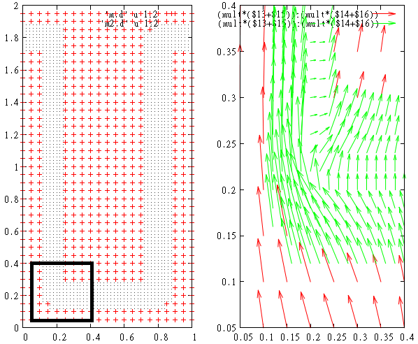
Multiple meshes
Generally, higher mesh resolution is required around the pn-junction interface since carriers concentration change significantly there. We already showed how it can be achieved by varying mesh step in chosen directions. Here we show another approach which consists in simultaneous using of multiple meshes with different resolutions.
Let’s consider our previous example with multilayer cell. We will change mesh step from 0.02 to 0.05 there, and add local mesh with mesh step 0.05 / 2.5 = 0.02. We make this local mesh as a main mesh around pn-junction, assigning higher priority to it. Priority is the third argument of the function AddMesh. Its default value is 0 (priority of default mesh is 0).
// valtype dz=.02;
valtype dz=.05;

// here we have previous code with specifying calculated volume and resolution

valtype nun=2.5; // using smaller mesh step around p-n junction

RegionUnion<3> *reg = new RegionUnion<3>();

reg->AddRegion(GetBox(Vector_3(-1,-left_length/2,length-w+dz),Vector_3(1,left_length/2,length-w-dz)));
for(int i=0;i<hp;i+=2){
 reg->AddRegion(GetBox(Vector_3(-1,i*a/2+left_length/2-dy,length-w),
   Vector_3(1,i*a/2+left_length/2+dy,w)));
 reg->AddRegion(GetBox(Vector_3(-1,i*a/2+left_length/2,w+dz),
   Vector_3(1,i*a/2+a-left_length/2,w-dz)));
}
for(int i=1;i<hp;i+=2){
 reg->AddRegion(GetBox(Vector_3(-1,(i+1)*a/2-left_length/2-dy,length-w),
   Vector_3(1,(i+1)*a/2-left_length/2+dy,w)));
 reg->AddRegion(GetBox(Vector_3(-1,(i+1)*a/2-left_length/2,length-w+dz),
   Vector_3(1,(i+1)*a/2+left_length/2,length-w-dz)));
}

// put local mesh with higher resolution and priority 1 inside region reg
task.AddMesh(Vector_3(0,dy,dz)/nun,reg,1);

task.DumpMeshes(1|3); // to see values of calculated variables at mesh nodes
Each mesh stores only nodes used in calculation.
gnuplot> p 'm.d', 'm2.d' lt -1 w d
This is photocurrent distribution for mesh nodes which are close to pn-junction
gnuplot> p [.05:.4][.05:.4] 'm.d' u 1:2:(mult*($13+$15)):(mult*($14+$16)) w vec
gnuplot> rep 'm2.d' u 1:2:(mult*($13+$15)):(mult*($14+$16)) w vec
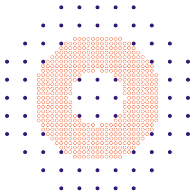
Note that local mesh can be placed in the region of arbitrary curved shape (not necessarily rectangular). This region can be an aggregation of not-connected sub-regions as well. Arbitrary number of meshes can be used at the same time.
This is an example of multiple meshes which we use in 3D modeling of on nanowires.
Nanowire. Using radial coordinates
Nanowires can be used as an alternative to thin film cells. One advantage is the use of radial junction geometry where light absorption and carrier collection are decoupled. This idea is the same as for multilayer geometry. A second advantage is that nanowire arrays can be designed to have very low reflectance and efficiently absorb incident light.
Here we show how to simulate nanowires using Microvolt. As in previous sections, we specify generation by scLambertSpectrum. This allows reduce dimensionality of the problem from 3D (x, y, z) to 2D (r, z). In general, for periodic arrays of nanowires, generation rate is almost symmetric under rotations, and calculation can be done in 2D as well.
We use our previous setup for multilayers and simulate half of the period. We also use insulator boundary conditions instead of periodic boundary conditions.
//  int hp=2; // number of half-periods in calculated box
//  task.SetPeriodicBoundaries(0x2);

 int hp=1; // number of half-periods in calculated box

 // y is a radial coordinate, hp*a/2+r is coordinate of the radial axis,
 // we consider negative radial values
 task.SetRadialCoordinate(1,hp*a/2,false);

 valtype sri=1e2; // insulator surface recombination, cm/sec
 Region_3 *LR = GetHalfSpace(Vector_3(0,-1,0),VEC_ZERO);
 task.AddReflectiveBoundary(LR,sri,sri,-1);
This is the resulted photocurrent distribution (we duplicated the result for positive radial values).
gnuplot> p [0:1][0:2.5] 'd.d' u 1:2:(mult*($13+$15)):(mult*($14+$16)) w vec
gnuplot> rep 'd.d' u (1-$1):2:(-mult*($13+$15)):(mult*($14+$16)) w vec
Note that current density is more concentrated close to the axis of the nanowire as it should be for our radial geometry.
3D textured film
Absorption enhancement can be achieved by texturing cell surface that provides antireflective and light trapping mechanisms for the incident light. Here we consider textured film drilled by square array of conical holes filled with silica.
int main(int argc,char **argv){

 string dir; // output directory
 if(scInit(argc,argv,dir)<0)
 return -1;

 valtype length=1; // film thickness
 valtype a=.6; // period of square lattice
 valtype R=.25; // cones radius
 valtype h=.8; // cones height
 valtype pn=.5; // pn-junction position
 valtype left_dop=1e18; // doping concentration of the left medium
 valtype right_dop=-1e18; // doping concentration of the right medium

 scMediumFactory med=getscSi(); // medium
 med.L[0]=100; // diffusion length
 valtype sr=VEC_INFTY; // contacts surface recombination
 valtype sri=0; // insulator surface recombination

 valtype dz=.02; // mesh step

 Vector_3 sz(a,a,length); // use it for 3D
//  Vector_3 sz(0*a,a,length); // use it for 2D

 scExperiment task(0,sz);
 task.SetResolution(dz);

 med.dop=left_dop;
 task.AddMediumRegion(med,GetHalfSpace(-Vector_3(0,0,1),pn));
 med.dop=right_dop;
 task.AddMediumRegion(med,GetHalfSpace(Vector_3(0,0,1),pn));

 task.SetPeriodicBoundaries(0x1|0x2);

 Region_3 *cone=GetPyramida(Vector_3(sz[0]/2,sz[1]/2,0),Vector_3(sz[0]/2,sz[1]/2,h),
 Vector_3(1,0,0),Vector_3(0,1,0),GetRegularPolygon(0,R,100));

 task.AddReflectiveBoundary(cone,sri,sri,1);

 task.AddContact(GetHalfSpace(-Vector_3(0,0,1),VEC_ZERO),sr,sr); // top contact
 task.AddVoltageContact(GetHalfSpace(Vector_3(0,0,1),length-VEC_ZERO),sr,sr); // bottom contact

 scGeneration *genAM = new scLambertSpectrum(Plane_3(Vector_3(0,0,1),0),spectra_dir.c_str(),
 "am1.5.in","si.nk",350,1240.8/med.Eg);
 task.AddGeneration(genAM);

 task.AddDetector("d",Vector_3(sz[0]/2,0,0),Vector_3(sz[0]/2,sz[1],sz[2]),INT_INFTY);
 task.AddDetector("d3d",Vector_3(0,0,0),Vector_3(sz[0],sz[1],sz[2]),iVector_3(6,6,10));
 task.AddFluxPlane("j",2,length/2);

 task.SetFluxIV("j"); // I-V calculation

 task.Calculate(.02);

 return 1;
}
Note that this example can be used for 2D simulation of a film drilled by triangular grooves as well.
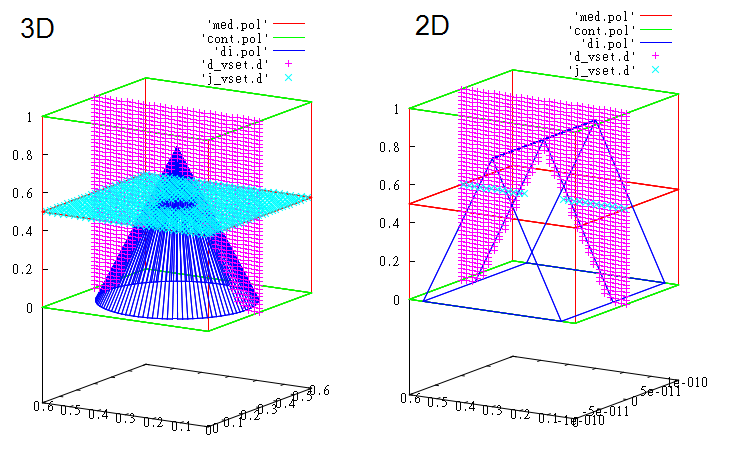
It could be helpful to look at specified geometry in gnuplot.
For this purpose you can use auxiliary files which are created before calculation:
- med.pol – medium regions
- cont.pol - contacts
- di.pol – insulator interface
- files with extension _vset.d - detectors.
Extension 'pol' in file name means that file stores polyhedra, d - dots.
For 3D and 2D textured films you will see
gnuplot> sp 'med.pol' w l, 'cont.pol' w l, 'di.pol' w l, 'd_vset.d', 'j_vset.d'
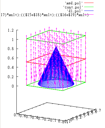
This is the calculated photocurrent distribution
gnuplot> mult=10
gnuplot> sp 'med.pol' w l, 'cont.pol' w l, 'di.pol' w l, \
gnuplot> 'd3d.d' u 1:2:3:(($14+$17)*mult):(($15+$18)*mult):(($16+$19)*mult) w vec
Substituting carriers’s generation from electromagnetic simulation
Until now we considered simple generation profile derived from Lambert-Beer law. However, it works only for planar case. For nanostructured devices you need to use independent electromagnetic simulation. It can be FDTD, Finite Elements, Transfer Matrix or any other method. For example, in standard FDTD scheme, plane wave impulse is directed onto the structure, the fields are recorded, transformed to the frequency domain and normalized to the incident spectrum, to calculate the absorption at each point r inside the structure:
\(\displaystyle \alpha(\omega, {\bf r}) = \frac{\omega \cdot {\rm Im}(\varepsilon) \left|{\bf E}(\omega,{\bf r})\right|^2}{c \cdot {\rm Re}\left[{\bf E}_{\rm inc}(\omega,{\bf r}),{\bf H}^*_{\rm inc}(\omega,{\bf r})\right]}\).
Here c is speed of light in vacuum, and \(\omega\) is frequency of light.
Generation rate is obtained by integration of calculated absorption \(a(\lambda, {\bf r})\) with incident solar Air Mass 1.5 Global Spectrum intensity \(I(\lambda)\) over the chosen wavelength range:
\(G({\bf r}) = \int_{\lambda_{\rm min}}^{\lambda_{\rm min}} \frac{\lambda}{hc} I(\lambda) a(\lambda, {\bf r}) d\lambda\).
Here wavelength \(\lambda = \frac{2\pi c}{\omega}\), h is the Planck's constant.
Generation rate data should be stored in some text or binary file. This file can be used as an input to Microvolt. For this purposes you can use class scGenerationTable
Here we present an example for silicon nanowires with height h = 2 μm, radius R = 200 nm, and distance of the pn-interface from the outer side of the nanowire d = 100 nm. The nanowires are arranged in a square lattice with period a = 800 nm and embedded in silica (refractive index n = 1.5) up to their top surface. There is no back-reflector below nanowires, and the region above the structure is air..
We calculated in FDTD reflectance-transmittance-absorption spectra, and generation rate (integrated wavelength range is 350–1100 nm), see results. We used EMTL software for FDTD. FDTD mesh step was 10nm.
Below you can see below the absorption profile inside the nanowire for the chosen wavelengths (max = 10 (μm)−1) and the corresponding generation rate (max = 1010 (μm)−3s−1); angular averaging is performed.

This is the Microvolt code for nanowire simulation with generation profile substituted from FDTD output file 'abs_3d.d'.
int main(int argc,char **argv){

 string dir; // directory for output files
 if(scInit(argc,argv,dir)<0)
   return -1;

 valtype R=.2; // nanowire radius
 valtype h=2; // nanowire height
 valtype uw=.1, dw=.1; // uw,dw - pn-junction distance from contact
 valtype pn=R/2; // pn-junction distance from nanowire surface
 valtype ndop=1e18; // n-doping
 valtype pdop=1e18;
 valtype L=.2; // diffusion length, um
 valtype sr=1e5; // contact surface recombination, cm/sec
 valtype sri=0; // insulator surface recombination, cm/sec

 valtype dx=.004; // mesh step along x-axis
 valtype nz_mult=1; // ratio dz/dx
 int rad=1; // use radial coordinates
 int nx; // number of mesh points per 2*R
 nx=int(acdiv(2*R,dx));
 int nz=int(acdiv(h,nz_mult*dx)); // number of mesh points per h

 scMediumFactory top=getscSi(); // silicon
 top.L[0]=L; // um
 scMediumFactory down=top;
 top.dop=ndop; down.dop=-pdop;

 // calculated box.
 Vector_3 p1(-R-dx,-R-dx,0), p2(R+dx,R+dx,h);
 if(rad)
   p1[1]=p2[1]=0; // y-axis is not working
 scExperiment task(p1,p2);
 task.SetResolutionN(iVector_3(nx+2,nx+2,nz));
 if(rad)
   task.SetRadialCoordinate(0,0,0); // x is radial axis

 Cylinder<Circle> *OC = GetCylinder(0,Vector_3(0,0,1),R-1e-10);
 Inverse<Region_3> *IOC = new Inverse<Region_3>(make_mngarg((Region_3 *)OC)); // outer cylinder
 Polyhedron_3 *DP=GetHalfSpace(Vector_3(0,0,-1),Vector_3(0,0,1e-10)); // bottom plane
 Polyhedron_3 *UP=GetHalfSpace(Vector_3(0,0,1),Vector_3(0,0,h-1e-10)); // top plane

 task.AddReflectiveBoundary(IOC,sri,sri,-3); // outer cylinder is insulator boundary
 task.AddVoltageContact(DP,sr,sr,VEC_INFTY,-1); // bottom plane is contact
 task.AddContact(UP,sr,sr,VEC_INFTY,-1); // top plane is contact
 ConfinedRegion<Cylinder<Circle> > *pnC = GetCylinder(0,Vector_3(0,0,1),R-pn,h-uw);

 task.AddMediumRegion(down,pnC); // p-region
 task.AddMediumRegion(down,GetHalfSpace(Vector_3(0,0,-1),Vector_3(0,0,dw)),1); // p-region
 if(accomp(dw,h-uw))
   task.AddMediumRegion(top,GetHalfSpace(Vector_3(0,0,1),Vector_3(0,0,dw)),1); // n-region
 Inverse<Region_3> *IpnC = new Inverse<Region_3>((Region_3 *)pnC);
 task.AddMediumRegion(top,IpnC); // n-region

 const char *fname="abs_3d.d"; // file with fdtd results
 string fdtd_dir; // directiry with this file
 // linear transformation between FDTD and Microvolt coordinate system
 Basis_3 bs(Vector_3(1,0,0),Vector_3(0,1,0),Vector_3(0,0,-1));
 valtype a=.8; // period of the nanowires array in FDTD
 Vector_3 shift(a/2,a/2,-h); // shift between FDTD and Microvolt coordinate systems
 // coordinates are in 0,1,2 columns; generation is in 3 column
 // 3 coordinates are used (3D).
 // FDTD output generation is in 1/sec/m/m/um; while Microvolt input generation is in 1/sec/m3.
 // to compensate for this, we use 1e6 factor
 scGeneration *gen=new scGenerationTable(fdtd_dir.c_str(),fname,iVector_3(0,1,2),3,3,bs,shift,1e6);
 gen = new scGenerationCylinder(make_mngarg(gen),2,0,64);
 task.AddGeneration(gen);

 // detectors resolution
 valtype detx=.2, detz=.05;
 task.AddDetector("d",p1,p2,Vector_3(detx,detx,detz));
 // task.AddDetector("yz",p1,p2,Vector_3(0,detx,detz));
 // task.AddDetector("xz",p1,p2,Vector_3(detx,0,detz));

 Vector_3 j0(-R-dx,-R-dx,h/2), j1(R+dx,R+dx,h/2);
 task.AddBoxDetector("j",j0,j1,iVector_3(nx+2,nx+2,1),BOX_BACK_Z);
 task.SetFluxIV("j");

 task.Calculate(.025);
 return 1;
}
Note that we can switch between 3D and 2D radial coordinates using flag rad. We also use angular averaging for generation rate in order to facilitate using 2D radial scheme. Generation FDTD table is substituted to Microvolt using class scGenerationTable.
We used different coordinate systems in FDTD and Microvolt. In Microvolt, nanowire axis passes coordinates origin, and nanowire bottom and top z-coordinates are 0 and h, correspondingly. In FDTD, nanowire axis pass the point x=a/2, y=a/2, and nanowire bottom and top z-coordinates are h and 0. To make linear transformation and shift between these two coordinate systems, we use parameters Basis_3 and Vector_3 in scGenerationTable constructor.
This is resulted IV-curve. This is resulted IV-curve. We normalize current on the area of the one period of the structure with single nanowire, a2.

Generation table can be specified in 1D or 2D (not only 3D, as above). For example, in our first case with 1D diode we used scLambertSpectrum to specify generation. Results of the simulation (including generation) were recorded in the output file ‘d.d’. We can repeat the simulation using generation recorded at this file and find that results will be the same:
 // valtype wv1 = 350; // shortest wavelength that enters the cell
 // valtype wv2 = 1240.8/left_med.Eg; // wavelengths that corresponds to silicon bandgap
 // scGeneration *gen = scLambertSpectrum(Plane_3(n,0),spectra_dir,"am1.5.in","si.nk",left_med.Eg);
 // task.AddGeneration(gen);

 Basis_3 bs(Vector_3(0,0,1),Vector_3(0,1,0),Vector_3(1,0,0));
 // last argument is 1e6, since in Microvolt output generation is in [1/sec/cm3],
 // while scGenerationTable reads generation in [1/sec/m3]
 scGeneration *gen=new scGenerationTable("","d.d",0,10,1,bs,0,1e6);
 task.AddGeneration(gen);
Organic solar cells
This part of the code is under development, We are happy for any collaboration from your side (please contact Alexei Deinega, deinega@yahoo.com).