Microvolt
is free C++ program for semiconductor devices modeling (diodes, solar cells, transistors etc.). Code can be compiled on UNIX and Windows. Currently we are extending Microvolt for organic solar cells.
How does it work?

Poisson and current continuity equations are discretized using finite-difference method in 1D, 2D, 3D, and cylindrical coordinates. Resolution of rectangular mesh can vary along each direction. Multiple meshes with different resolution can be used at the same time. Architecture of the code allows easily include other types of meshes.
To solve system of discretized equations we use Newton-Rhapson method. Linear algebra operations can be performed using PARDISO, LAPACK or any other solvers.
For solar cells modeling, one can use carriers generation profile obtained from independent electromagnetic simulation. We are using results obtained by EMTL package that can be substituted as an input to Microvolt.
Application of the code
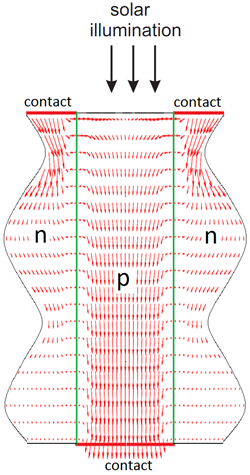
Microvolt was successfully used to simulate solar cells of different geometries (nanowires, textured thin films) based on Si, GaAs, CdTe, etc. This is list of chosen publications:
- A. Deinega, S. Eyderman, S. John, "Coupled optical and electrical modeling of solar cell based on conical pore silicon photonic crystals", J. Appl. Phys. 113, 224501 (2013). ABSTRACT PDF
- A. Deinega and S. John, "Solar power conversion efficiency in modulated silicon nanowire photonic crystals", J. Appl. Phys. 112, 074326 (2012). ABSTRACT PDF
- A. Deinega and S. John, "Finite difference discretization of semiconductor drift-diffusion equations for nanowire solar cells", Comp. Phys. Comm. 183, 2128 (2012). ABSTRACT PDF
Nanostructured solar cells
Crystalline silicon is the most widely used semiconductor in photovoltaics technology due to its abundance, nontoxicity and good matching between its electronic bandgap and the solar spectrum. Silicon is an indirect-bandgap semiconductor with relatively low absorption in the near infrared. To compensate the wide variation of absorption length with wavelength, the thickness of silicon solar cells has typically been hundreds of microns. This leads to cost issues since commercial high quality silicon is required to extend the carrier diffusion length to collect generated carriers before they can recombine.
Thin film cells technology is one possible direction to reduce the cost, using a thin absorber layer. Since carriers only have to be collected within a distance of a film thickness, poor quality silicon can be used. However, the efficiency of such cells is low because of significant reduction in light absorption. While typical efficiency of commercially available wafer-based silicon solar cells is 15-20%, the best efficiency of thin-film silicon solar cells is around 10%.
Traditional methods to increase absorption inside solar cell include the use of antireflective quarter-wave layers or texturing of thin films by nanocones or nanoholes. In a long wavelength regime textured structure acts like gradient index film with a low reflection while at the short wavelength regime suppression of the reflection is achieved by the entanglement of the rays multiply refracted and reflected by the texture. For the visible range, the textured surfaces with the periodicity of the order of optical wavelength are highly efficient. Recently antireflective properties of textured surface in a whole range of size-to-wavelength ratios, including effective medium and geometric optics regimes, were studied.
Another effect achieved by cell surface texturing is the trapping of the light entered the cell. Traditionally light trapping was considered as a geometrical optics effect based on random scattering of the rays from the texture. This scattering results on increase of the effective path length by a factor of 4n2 and therefore better absorption. Recently it was shown that light trapping in a wave optics regime could be more pronounced.
Another promising architecture consists of silicon nanowires. Here, one advantage is the use of a radial junction geometry where light absorption and carrier collection are decoupled, greatly increasing collection efficiency for silicon of poor quality. A second advantage is that silicon nanowire arrays can be designed to have very low reflectance and efficiently absorb incident light. Recently, sinusoidaly modulated nanowires were proposed as a combination of nanowire and 3D photonic crystal geometries. Such modulation can lead to strong light trapping effects due to the phenomenon of parallel interface refraction.
Nanostructuring of the solar cell gives opportunities for nontrivial choice pn-junction and contacts location. For example, radial junction geometry can be used for nanowires. It can greatly increase efficiency for silicon of poor quality due to decoupling of a light absorption and carrier collection directions. To calculate efficiency for nanostructured cells one need to combine electromagnetic and electrical modeling. Electromagnetic part is used to calculate absorption inside the structure and charges generation profile. This profile should be substituted as an input for electrical modeling to calculate solar cell efficiency with consideration of bulk and surface recombination losses.


