Model
Here we very briefly review physics of semiconductor devices and numerical methods for their modeling.
We recommend following books for more detailed introduction:
- D. Neamen, Semiconductor Physics and Devices, McGraw-Hill (2003)
- Jenny Nelson, The physics of solar cells, Imperial College Press (2003)
- S. Selberherr, Analysis and Simulation of Semiconductor Devices, Springer (1984).
- R. Kircher and W. Bergner, Three-Dimensional Simulation of Semiconductor Devices, Birkhauser Verlag (1991).
There are also some good sources online:
Some definitions
Intrinsic electrons and holes concentration ni can be calculated as
\(\displaystyle n_{i}^{2}={{N}_{C}}{{N}_{V}}{{e}^{-\frac{{{E}_{g}}}{kT}}}\),
where NV и NC are effective densities of states in conduction and valence bands. Their values can be found as
\(\displaystyle {{N}_{C,V}}=2{{\left( \frac{2\pi m_{n,p}^{*}kT}{{{h}^{2}}} \right)}^{3/2}}\),
where \(m_{n,p}^{*}\) are electron and hole effective masses.
In doped semiconductor equilibrium electrons and holes concentrations n0, p0 can be calculated as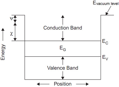
\({{n}_{0}}{{p}_{0}}=n_{i}^{2}\)
\({{n}_{0}}+{{N}_{A}}={{p}_{0}}+{{N}_{D}}\),
where ND and NA are concentrations of ionized donors and acceptors.
These relations lead to
\({{n}_{0}}=\frac{({{N}_{D}}-{{N}_{A}})}{2}+\sqrt{{{\left( \frac{{{N}_{D}}+{{N}_{A}}}{2} \right)}^{2}}+n_{i}^{2}}\)
\({{p}_{0}}=\frac{n_{i}^{2}}{{{n}_{0}}}\)
In general, electrons and holes concentrations can be calculated as
\(n = {n_i}\exp \left( {\frac{{{E_n} - \left( {{E_i} - q\psi } \right)}}{{kT}}} \right) \)
\(p = {n_i}\exp \left( {\frac{{\left( {{E_i} - q\psi } \right) - {E_p}}}{{kT}}} \right) \)
where EF,n and EF,p are quasi-Fermi levels for electrons and holes, and \(\left( {{E_i} - q\psi } \right)\) is intrinsic Fermi level. If electrostatic potential \(\psi = 0\) then intrinsic Fermi level is equal to \({E_i} = - \chi - \frac{{{E_g}}}{2} + \frac{1}{2}kT\ln \left( {\frac{{{N_v}}}{{{N_c}}}} \right)\), where \(\chi\) is electron affinity and Eg is bandgap.
Semiconductor bulk equations
To model semiconductor device we need to solve Poisson equation and continuity equations for electrons and holes
\(\nabla \left( {\varepsilon \nabla \psi } \right) = - q(p - n + N_D^{} - N_A^{}) \)
\(\nabla {J_n} = -q(G - R) \)
\(\nabla {J_p} = q(G - R) \)
where \(\psi\) is electrostatic potential, n and p are electron and hole densities, \(\varepsilon\) is dielectric function, Jn,p are current densities, G and R are generation and recombination rates.
Current densities are expressed as
\({J_n} = {\mu _n}n\nabla {E_n}\)
\({J_p} = {\mu _p}p\nabla {E_p}\)
where \(\mu_{n,p}\) are mobilities. They are related to diffusion coefficients Dn,p by Einstein relation \({D_i} = {\mu _i}kT\).
Taking into account relation between concentrations and quasi-Fermi levels we get
\({J_n} = - {\mu _n}n\nabla (q\psi - {E_i} - \ln {n_i}) + q{D_n}\nabla n\)
\( {J_p} = - {\mu _p}p\nabla (q\psi - {E_i} - \ln {n_i}) - q{D_p}\nabla p\)
In the case of homo-junction (ni and Ei are constants) we have
\({J_n} = - q{\mu _n}n\nabla \psi + q{D_n}\nabla n\)
\({J_p} = - q{\mu _p}p\nabla \psi - q{D_p}\nabla p\)
Generation rate G is produced by light absorption and can be calculated from independent electromagnetic simulation.
Recombination rate is a sum of following terms:
Radiation recombination \(R = B(np - {n_0}{p_0})\)
Auger recombination \(R = {C_n}n(np - n_0^{}{p_0}) + {C_p}p(np - n_0^{}p_0^{})\)
Shockley-Read-Hall recombination through defect levels (traps)
\(\displaystyle R = \frac{{(np - {n_0}{p_0})}}{{{\tau _p}(n + {n_1}) + {\tau _n}(p + {p_1})}}\)
Meaning of all recombination parameters can be easily found in literature.
Boundary conditions
Semiconductor-metal interface
Potential is calculated as
\(q\psi = V - \left( {{\phi _s} - {\phi _{s0}}} \right) - {\phi _B}\)
Here V is applied voltage,
\({\phi _s} = -{E_i} - {\psi _{bi}} = \chi + {\phi _n}\) is semiconductor workfunction (distance between vacuum level and equilibrium Fermi level),
\(\displaystyle {E_i} = -\chi - \frac{{{E_g}}}{2} + \frac{1}{2}kT\ln \left( {\frac{{{N_v}}}{{{N_c}}}} \right)\) is intrinsic equilibrium Fermi level,
\(\displaystyle {\psi _{bi}} = kT\ln \frac{{{n_0}}}{{{n_i}}} = -kT\ln \frac{{{p_0}}}{{{n_i}}}\) is distance between equilibrium Fermi level and intrinsic equilibrium Fermi level,
\(\displaystyle {\phi _n} = -kT\ln (\frac{{{n_0}}}{{{N_C}}})\) is distance between conduction band and equilibrium Fermi level,
\({\phi _{s0}}\) is semiconductor workfunction for some reference medium (if this is the same medium with zero doping then \({\phi _s} - {\phi _{s0}} = -{\psi _{bi}}\)),
\({\phi _B} = {\phi _m} - {\phi _s}\) is Schottky potential barrier at the contact (it is equal to zero for Ohmic contact),
\({\phi _m}\) is metal workfunction.
Boundary conditions for current are
\(\overrightarrow {{J_n}} \cdot \overrightarrow {\text{n}} = q{s_n}\left( {n - {n_1}} \right) \)
\(\overrightarrow {{J_p}} \cdot \overrightarrow {\text{n}} = -q{s_p}\left( {p - {p_1}} \right) \)
where \(\overrightarrow {\text{n}} \)is normal vector to the surface, sn, sp are electrons and holes recombination velocities, n1 and p1 are equilibrium electrons and holes concentrations at surface:
\(\displaystyle {n_1} = {n_0}\exp \left( { - \frac{{{\phi _B}}}{{kT}}} \right) = {N_C}\exp \left( {\frac{{ - {\phi _n} - {\phi _m} + {\phi _s}}}{{kT}}} \right) = {N_C}\exp \left( {\frac{{\chi - {\phi _m}}}{{kT}}} \right) \)
\(\displaystyle {p_1} = {p_0}\exp \left( {\frac{{{\phi _B}}}{{kT}}} \right) = {N_V}\exp \left( {\frac{{ - {E_g} + {\phi _n} - \chi - {\phi _n} + {\phi _m}}}{{kT}}} \right) = {N_V}\exp \left( {\frac{{{\phi _m} - \chi - {E_g}}}{{kT}}} \right) \)
For infinite surface recombination we have
\(n = {n_1} \)
\(p = {p_1} \)
In the case of Schottky contact, \({\phi _B} > 0\) for n-doped semiconductor and \({\phi _B} < 0\) for p-doped semiconductor.
In the case of Ohmic contact, metal and semiconductor workfunctions are assumed to be equal, \({\phi _B} = 0\). Therefore equilibrium surface values of concentration are equal to equilibrium values at the bulk n1 = n0 and p1 = p0.
Semiconductor-insulator interface
In the case of no surface charges at the surface we put normal component of the electric field to be zero:
\(\vec \nabla \psi \cdot \vec n = 0\)
Boundary conditions for current are
\(\overrightarrow {{J_n}} \cdot \overrightarrow {\text{n}} = -\overrightarrow {{J_p}} \cdot \overrightarrow {\text{n}} = q{R_{surf}}\)
where recombination at the interface is expressed similar to Shockley-Read-Hall recombination:
\(\displaystyle {R_{surf}} = \frac{{(np - {n_0}{p_0})}}{{s_p^{ - 1}(n + {n_1}) + s_n^{ - 1}(p + {p_1})}}\)
Here sn, sp are electrons and holes recombination velocities, n1 and p1 have the same meaning as for SRH recombination.
In the case of zero surface recombination velocity, there is no current flow towards to the surface:
\(\overrightarrow {{J_n}} \cdot \overrightarrow {\text{n}} = \overrightarrow {{J_p}} \cdot \overrightarrow {\text{n}} = 0\)
Numerical method
Poisson and continuity equations can be discretized in finite differences, finite boxes or finite elements. The finite difference method is the simplest to implement. Discretization of Poisson equation and continuity equations is straightforward. Current in continuity equations is approximated using Scharfetter–Gummel scheme.
Finite difference method is very stable and leads to a system of nonlinear equations with simple Jacobian structure that can be efficiently solved by Newton's technique. However, this method is less flexible in varying of mesh resolution. To improve accuracy of the method one can use nonuiform mesh step along each dimension or multiple meshes with different resolution.
Discretization of semiconductor equations on a mesh leads to system of nonlinear equations which can be solved using multidimensional Newton's method. In one dimensional Newton's method, in order to solve equation \(f(x)=0\), you start with some initial guess x0 and iteratively move to solution \(x_{n+1} = x_n - \frac{f(x_n)}{f'(x_n)}\). This method is easily extended to more dimensions: \(J(x_n) \cdot \Delta x = -f(x_n)\), where J is the Jacobian matrix of f and \( \Delta x = x_{n+1} - x_n\). The iterative process is repeated until f(xn) will be small enough so we can consider xn as a solution.
System of discretized semiconductor equations contains three equations for each mesh point. Therefore a full Newton iteration corresponds to inversion of 3N × 3N matrix (N is number of mesh points). To speed up the process of convergence, one can solve different equations separately. For example, (1) make a few Newton iterations for continuity equations (2N × 2N matrix), (2) substitute calculated Fermi-levels into Poisson equation, (3) make a few Newton iterations for Poisson equation (N × N matrix), (4) substitute calculated potential to continuity equations and return to step (1).